Power transistors are one of the primary contributors to power loss in a switching power supply. Losses in the transistors are generally separated into two categories; conduction and switching. Conduction losses are those caused by current flow when the transistor is on and switching losses occur in the transition between on and off states.When on, GaN transistors (like those made of silicon) resemble a resistance between drain and source, often referred to as Ron, and the conduction losses are proportional to this resistance. A key benefit of GaN and other WBG materials is their relationship between breakdown voltage and Ron. Figure 1 shows the theoretical limits of this relationship for silicon, GaN, and silicon carbide (SiC), another WBG material. It can be seen that for a given breakdown voltage, the Ron of the WBG devices is much lower than that of silicon, with GaN being the lowest of the three. As silicon is nearing its theoretical limit, the use of GaN and other WBG materials becomes necessary if improvements to Ron are to continue.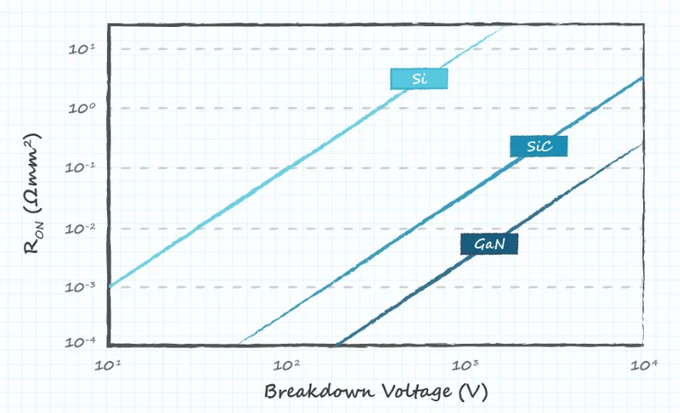
Figure 1: Theoretical limits of Ron vs. breakdown voltage for Si, GaN, and SiC transistors
In addition to improvements in conduction losses, the use of GaN also leads to a reduction in switching losses. There are multiple factors that contribute to switching losses, several of which are improved through the use of GaN. One loss mechanism results from the fact that the current in a transistor begins to flow before the drain-source voltage begins to fall, as shown in Figure 2. During this time, the losses (equal to the volt-amp product) are very large. Increasing the speed at which the switch turns on will reduce the losses incurred during this transition. Because GaN transistors are able to turn on faster than silicon transistors, they are able to reduce the losses caused by this transition.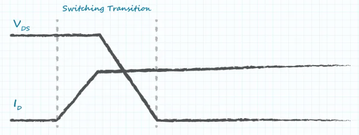
Figure 2: Drain Voltage and current waveforms during switching transition
Another way that GaN reduces switching loss is through the absence of a body diode. To avoid a short circuit condition, a period of time exists when both switches of a half-bridge are off, known as the ”dead-time”. During this period, current continues to flow, but because both switches are off, it is forced through the body diode. The body diode is much less efficient than the Ron resistance of a silicon transistor when it is on. For a GaN transistors there is no body diode. Current that would flow through the body diode of a silicon transistor instead flows through the Ron resistance. This significantly reduces the losses incurred during the dead-time.Because the body diode of a silicon transistor conducts during the dead-time, it must be turned off when the other switch turns on. During this time, current flows in the reverse direction as the diode turns off, causing additional losses. In a GaN transistors, the absence of a body diode results in near zero reverse recovery losses.


 Phone:+86-+86 137-2371-6834 Timber (WhatsApp)
 Tel:+86-0755-29665062
 Email:mkt1@jinruipower.com
 Add: No. 13A16 Huafeng International Commercial Building, No.4018 Bao’an Avenue, Xixiang, Baoan District, Shenzhen China


 Alibaba
 0755-29665062
 Online Service